A Technical Deep Dive into Semiconductor Architecture, Manufacturing, and the Future of Computing
Introduction: The Silicon Revolution That Changed Everything
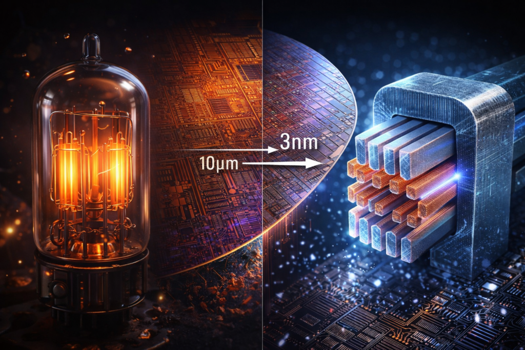
The modern world runs on sand—specifically, ultra-purified silicon crystals etched with patterns billions of times smaller than a human hair. The evolution of computer chips represents humanity’s most sophisticated manufacturing achievement, a journey from bulky vacuum tubes consuming kilowatts of power to multi-billion transistor architectures operating at the atomic scale.
This article provides a comprehensive technical examination of semiconductor evolution, from fundamental physics to cutting-edge 3nm Gate-All-Around (GAA) transistors, advanced packaging technologies, and post-silicon computing paradigms. Whether you’re a computer engineering student, a practicing VLSI designer, or a technology strategist, this deep dive offers the technical accuracy and architectural insights necessary to understand where computing has been—and where it’s headed.
Chapter 1: The Pre-Silicon Era (1940s–1950s)
1.1 Vacuum Tubes: The Thermionic Foundation
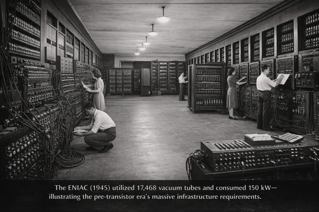
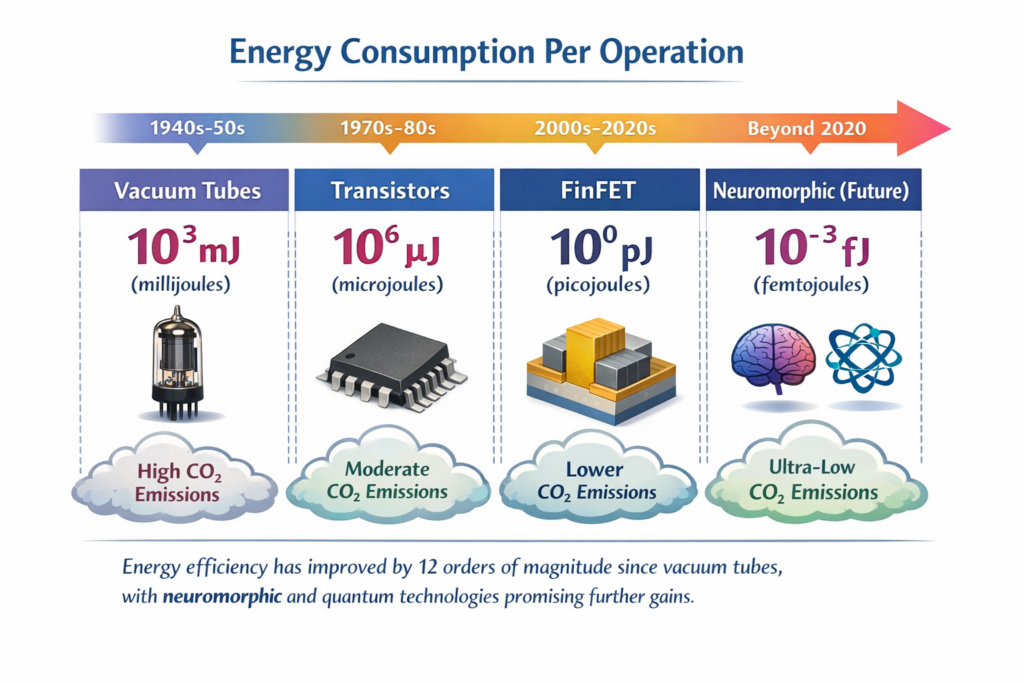
Before solid-state electronics, computing relied on vacuum tubes (thermionic valves)—glass envelopes containing heated cathodes that emitted electrons toward anodes, with control grids modulating current flow. The ENIAC (1945), the first general-purpose electronic computer, utilized 17,468 vacuum tubes, consumed 150 kW of power, and occupied 1,800 square feet.
Technical Limitations:
- Reliability: Mean time between failures (MTBF) of approximately 50 hours
- Switching speed: Limited to hundreds of kilohertz due to electron transit times
- Power consumption: Filament heating required continuous power dissipation
- Physical scale: Discrete component size prevented meaningful miniaturization
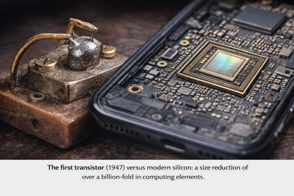
1.2 The Transistor Revolution (1947)
The invention of the point-contact transistor at Bell Labs by Bardeen, Brattain, and Shockley marked the dawn of solid-state electronics. Unlike vacuum tubes, transistors leveraged semiconductor physics—specifically the manipulation of electron and hole concentrations in germanium (later silicon) through P-N junctions.
Key Technical Innovation: The transistor operated as a voltage-controlled current source, replacing the thermionic emission mechanism with field-effect modulation. Early germanium transistors achieved current gains (β) of 20-50, with switching speeds orders of magnitude faster than vacuum tubes while consuming microwatts rather than watts.
Chapter 2: The Integrated Circuit Era (1958–1970s)
2.1 From Discrete to Integrated: Kilby and Noyce
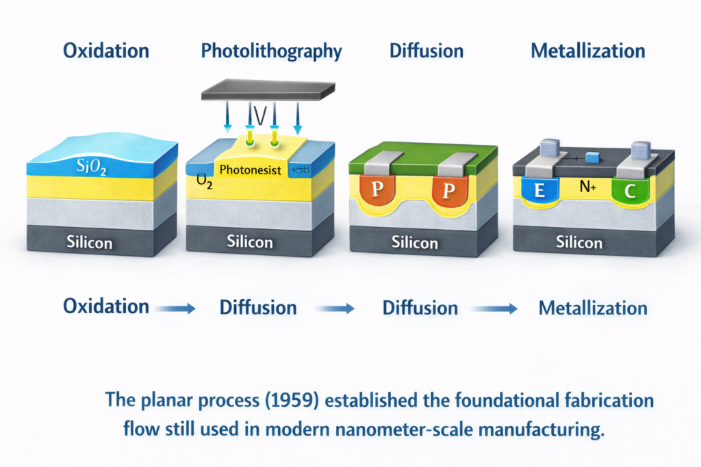
The conceptual leap from individual transistors to integrated circuits (ICs) solved the “tyranny of numbers”—the exponential reliability degradation as systems incorporated more discrete components. Jack Kilby’s 1958 germanium IC and Robert Noyce’s 1959 silicon monolithic IC (using photolithography and planar processing) established the fabrication paradigm still used today.
Planar Process Technical Details: Noyce’s Fairchild Semiconductor developed the planar process utilizing silicon dioxide (SiO₂) passivation layers. This technique:
- Created stable P-N junctions through thermal diffusion
- Enabled photolithographic pattern transfer with micron-scale resolution
- Provided surface passivation preventing contamination
- Allowed interconnection via evaporated aluminum metallization
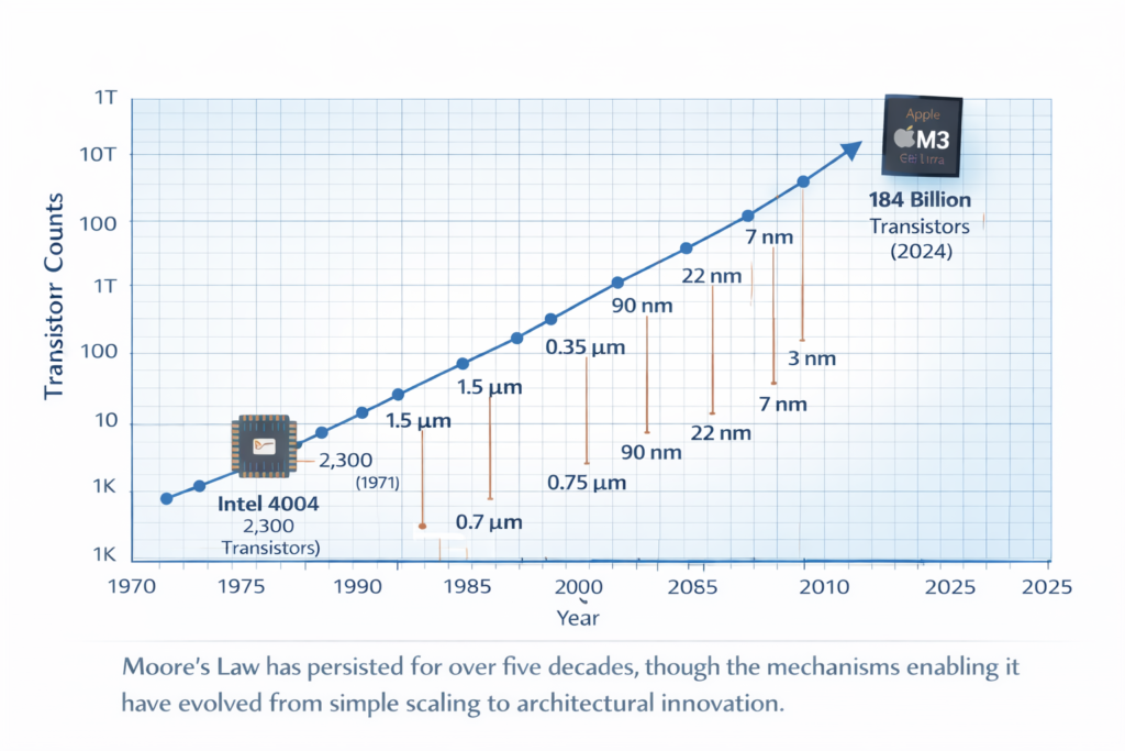
2.2 Moore’s Law: The Exponential Trajectory
In 1965, Gordon Moore observed that the number of components per integrated circuit was doubling approximately every year (later revised to every two years). This observation became a self-fulfilling prophecy driving semiconductor economics.
Mathematical Formulation:N(t)=N0⋅2t/2
Where N(t) represents transistor count at time t (in years), and N0 is the initial count. This exponential scaling required:
- Lithographic resolution improvements: From micrometers to nanometers
- Die size increases: From 1mm² to 800+ mm² for high-performance chips
- Yield management: Defect density reduction following Y=(1+DA)n1
Chapter 3: The Microprocessor Revolution (1971–1990s)
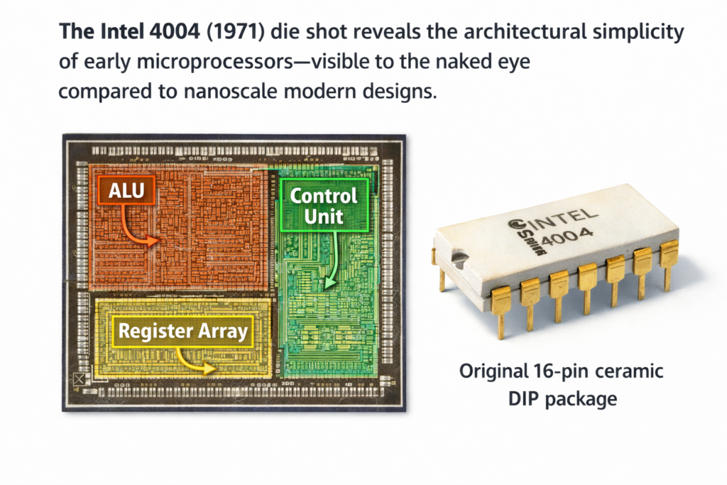
3.1 The Intel 4004: CPU on a Chip
The 4004, developed by Federico Faggin, Ted Hoff, and Stan Mazor, integrated a 4-bit CPU onto a single 12mm² die using 10μm PMOS technology. Its 2,300 transistors executed 60,000 instructions per second at 740 kHz—modest by modern standards, but revolutionary in integrating the central processing unit.
Architectural Significance:
- 4-bit word length: Limited address space to 4KB (with 8-bit instruction words)
- 16-pin DIP package: Constrained by packaging technology of the era
- PMOS logic: Required negative voltage supplies; superseded by NMOS then CMOS
3.2 From 8-bit to 32-bit: Architectural Evolution
The progression from 4004 to 8008 (8-bit, 1972), 8080 (1974), and 8086 (1978) established the x86 architecture dominating computing today. Key technical developments included:
Memory Segmentation (8086): The 20-bit address bus (1MB address space) used segment registers (CS, DS, SS, ES) with 16-bit offsets, creating the segmented memory model that plagued programmers until protected mode 32-bit architectures.
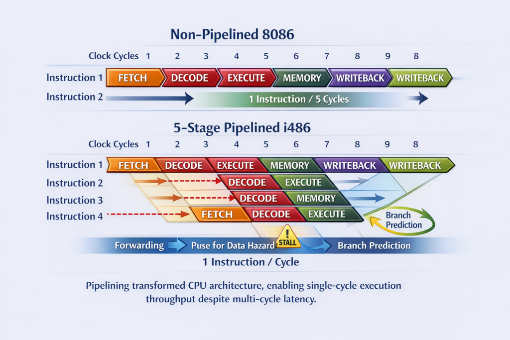
Pipelining and Caches (i486, 1989): The i486 introduced:
- 5-stage pipeline: Fetch, Decode, Execute, Memory, Writeback
- 8KB unified L1 cache: On-chip SRAM reducing memory latency
- Integrated FPU: Previously external 8087/80287/80387 coprocessors
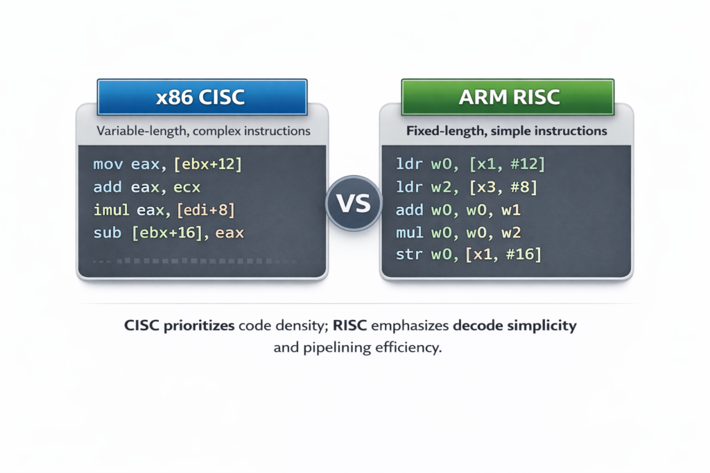
3.3 RISC vs. CISC: Architectural Philosophy
The 1980s witnessed the RISC (Reduced Instruction Set Computer) revolution led by David Patterson (Berkeley RISC, later SPARC and ARM) and John Hennessy (MIPS). This challenged the CISC (Complex Instruction Set Computer) orthodoxy of x86.
Technical Comparison:Table
| Feature | CISC (x86) | RISC (ARM/MIPS) |
|---|---|---|
| Instruction Length | Variable (1-15 bytes) | Fixed (32-bit typically) |
| Addressing Modes | Complex (e.g., base + index × scale + disp) | Simple (register + immediate) |
| Registers | 8 (legacy x86) to 16 (x86-64) | 32 general-purpose |
| Memory Access | Direct memory operands | Load/Store architecture only |
| Decoder Complexity | High (microcode translation) | Low (direct execution) |
Chapter 4: The Nanometer Era and Physics Challenges (1990s–2010s)
4.1 Sub-Micron Scaling and Quantum Effects
As process nodes shrank below 1μm (1000nm), classical semiconductor physics encountered quantum mechanical limitations:
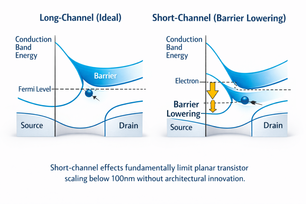
Short Channel Effects (SCE): When channel length L approaches the depletion region width, drain voltage modulates the barrier height, causing:
- Drain-Induced Barrier Lowering (DIBL): Threshold voltage (Vth ) reduction with drain voltage
- Subthreshold swing degradation: Inability to achieve steep on/off transitions
- Velocity saturation: Carrier velocity ceases increasing with electric field
The subthreshold swing limit (60 mV/decade at room temperature) became the fundamental constraint preventing voltage scaling.
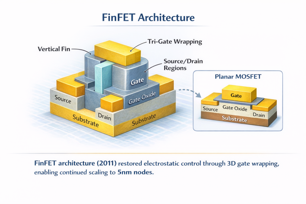
4.2 The FinFET Revolution (22nm–5nm)
Intel’s introduction of Tri-Gate transistors (FinFETs) at 22nm (2011) represented the most significant device physics innovation since the planar MOSFET. By raising the channel into a vertical “fin” surrounded by gate on three sides, FinFETs restored electrostatic control at nanometer scales.
FinFET Technical Specifications:
- Structure: Vertical silicon fin with height Hfin ≈ 30-50nm, width Wfin ≈ 5-8nm
- Gate control: Tri-gate (3-sided) electrostatic confinement
- Subthreshold swing: Improved to ~70 mV/decade (approaching 60 mV limit)
- Leakage reduction: Ioff improvements of 100× over planar
Manufacturing Complexity: FinFETs required:
- Self-aligned double patterning (SADP): For fin and gate definition
- High-k/metal gate (HKMG): Hafnium oxide (κ ≈ 25) replacing silicon dioxide
- Strained silicon: Germanium doping enhancing carrier mobility
4.3 Process Node Milestones and Lithography
The progression from 130nm to 7nm required revolutionary lithography:Table
| Node | Year | Key Technology | Lithography |
|---|---|---|---|
| 130nm | 2000 | Copper interconnects, low-k dielectrics | 248nm DUV |
| 90nm | 2003 | Strained silicon, immersion lithography | 193nm DUV |
| 45nm | 2007 | High-k/metal gate | 193nm immersion |
| 22nm | 2011 | FinFET (Tri-Gate) | 193nm multi-patterning |
| 14nm | 2014 | FinFET mature | 193nm quad-patterning |
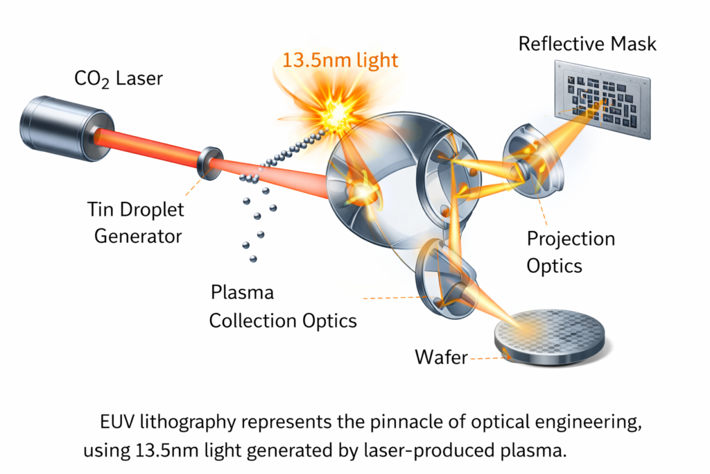
| 7nm | 2018 | EUV introduction | 13.5nm EUV |
Extreme Ultraviolet Lithography (EUV): EUV systems utilize 13.5nm wavelength light (produced by laser-produced tin plasma) reflected through Zeiss-designed multilayer mirrors (Mo/Si multilayers with 40-50 layer pairs). Each ASML NXE:3800E system costs >$300M and requires:
- Vacuum operation: EUV absorption by all materials
- Reflective optics: 6-mirror systems with 0.33 NA (0.55 NA for High-NA)
- Pellicle protection: Thin membranes protecting photomasks
Chapter 5: The Post-Moore Era: Advanced Architectures (2020s–Present)
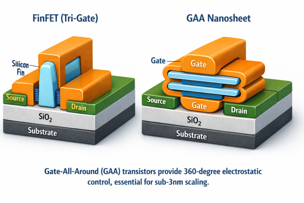
5.1 Gate-All-Around (GAA) Transistors
As FinFETs approached physical limits at 3nm, the industry transitioned to Gate-All-Around (GAA) transistors—specifically nanosheet or nanowire architectures where the gate completely surrounds the channel.
GAA Technical Advantages:
- Electrostatic control: 4-sided gate wrapping provides superior channel control versus FinFET’s 3-sided approach
- Continuous scaling: Enables sub-3nm nodes (2nm, 1.4nm roadmap)
- Subthreshold swing: Approaches ideal 60 mV/decade limit
- Current drive: Stacked nanosheets provide width flexibility without fin quantization constraints
Samsung MBCFET (Multi-Bridge Channel FET): Samsung’s 3nm process (2022) utilizes horizontal nanosheets with:
- 3-5 nanosheet stacks: Vertical stacking increasing drive current
- Sheet width Wsheet : 5-15nm tunable per device for Vth optimization
- Inner spacer technology: Reducing parasitic capacitance
- Performance claims: 23% performance improvement or 45% power reduction versus 5nm FinFET
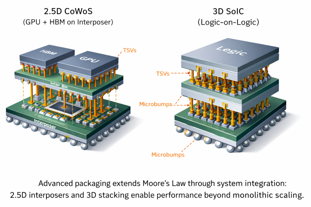
5.2 Advanced Packaging: More Than Moore
When transistor scaling slowed, the industry pivoted to “More Than Moore”—advanced packaging enabling system-level integration without node shrinkage.
2.5D Integration (CoWoS, EMIB):
- Silicon Interposers: Passive silicon dies with sub-micron wiring connecting multiple chips
- Through-Silicon Vias (TSVs): Vertical copper interconnects penetrating the substrate
- HBM (High Bandwidth Memory): 3D-stacked DRAM connected via interposer to GPUs/CPUs
- HBM3E specifications: 9.6 Gbps/pin, 1.2 TB/s bandwidth per stack
3D Integration (SoIC, Foveros): True 3D stacking places logic dies atop each other:
- Wafer-to-Wafer bonding: Copper-to-copper direct bonding at micron-scale alignment
- Face-to-face vs. face-to-back: Different thermal and TSV routing strategies
- Thermal challenges: 2× thermal resistance compared to 2D due to stacked heat sources
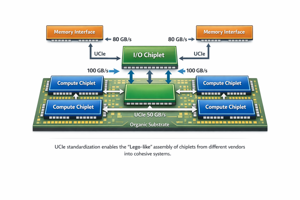
5.3 Chiplet Architecture and UCIe
The transition from monolithic SoCs to chiplet-based designs represents a paradigm shift in semiconductor economics.
Chiplet Advantages:
- Yield improvement: Yield=(1+αDefect⋅Area)−α — smaller dies have exponentially higher yields
- Process optimization: Compute chiplets at 3nm, I/O chiplets at mature nodes (cost optimization)
- IP reuse: Standardized chiplets across product lines
- Time-to-market: Parallel development of chiplets versus sequential monolithic design
UCIe (Universal Chiplet Interconnect Express): The UCIe 1.1 standard (2023) defines:
- Physical layer: Bump pitch options (25μm standard, 55μm advanced)
- Data rates: Up to 2 GT/s (NRZ) or 4 GT/s (PAM4) per pin
- Protocols: PCIe and CXL mapping for software compatibility
- Power efficiency: <0.5 pJ/bit for short-reach die-to-die
Chapter 6: Beyond Silicon: Post-CMOS Computing
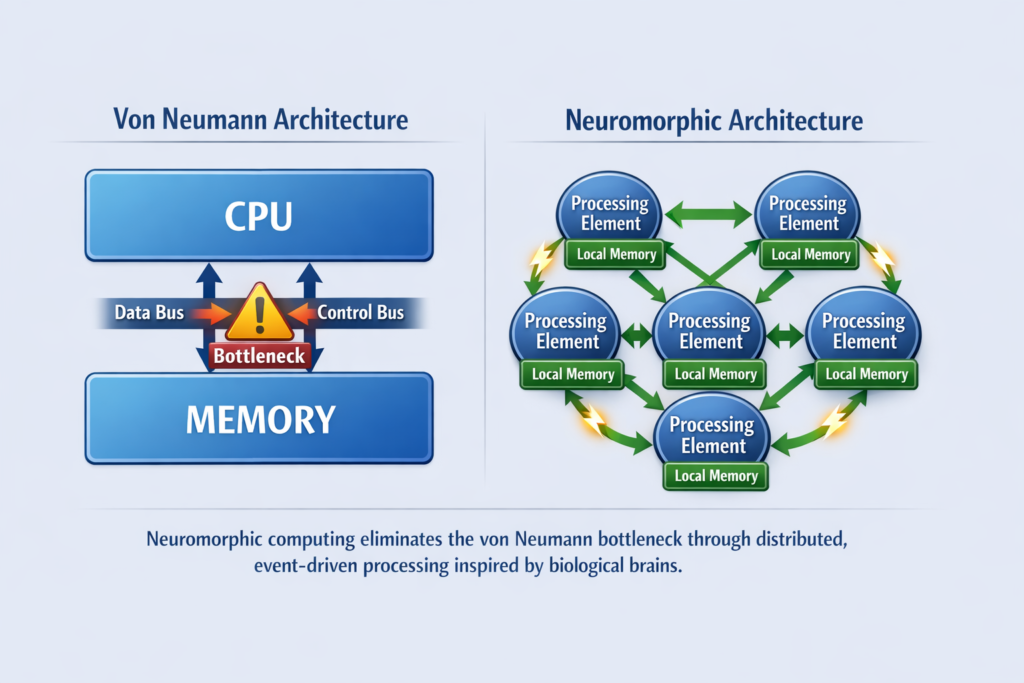
6.1 Neuromorphic Computing
Neuromorphic architectures mimic biological neural networks through event-driven, massively parallel processing. Unlike von Neumann architectures, neuromorphic chips co-locate computation and memory.
Intel Loihi 2 (2021):
- 128 neuromorphic cores: Each with 1,024 neurons
- Spiking Neural Networks (SNN): Event-driven computation (asynchronous)
- Process: Intel 4 (previously 14nm)
- Power efficiency: 10-100× improvement over GPUs for inference workloads
Memristor-Based Synapses: Phase-change memory (PCM) and resistive RAM (RRAM) implement analog synaptic weights:
- Multi-level cells: 4-6 bits per device representing synaptic strength
- In-memory computation: Ohm’s Law multiplication (I=V⋅G ) within memory arrays
- Challenges: Device variability, drift, and endurance limitations
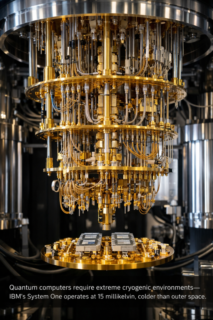
6.2 Quantum Computing
Quantum processors leverage superposition and entanglement for exponential speedup in specific problem domains.
Qubit Technologies:Table
| Technology | Coherence Time | Gate Fidelity | Operating Temp |
|---|---|---|---|
| Superconducting | 100-500 μs | 99.5% | ~15 mK |
| Trapped Ion | 1-10 s | 99.9% | Room temp (ions) |
| Photonic | N/A (flying qubits) | 99% | Room temp |
| Silicon Spin | 1-30 ms | 99% | ~1 K |
IBM Quantum Roadmap:
- Condor (2023): 1,121 superconducting qubits
- Flamingo (2025): 5,000+ qubits with error correction
- Kookaburra (2029): 100,000 qubits, fault-tolerant systems
Challenges:
- Decoherence: Environmental noise destroying quantum states
- Error correction: Surface codes requiring 1,000+ physical qubits per logical qubit
- Cryogenic infrastructure: Dilution refrigerators limiting scalability
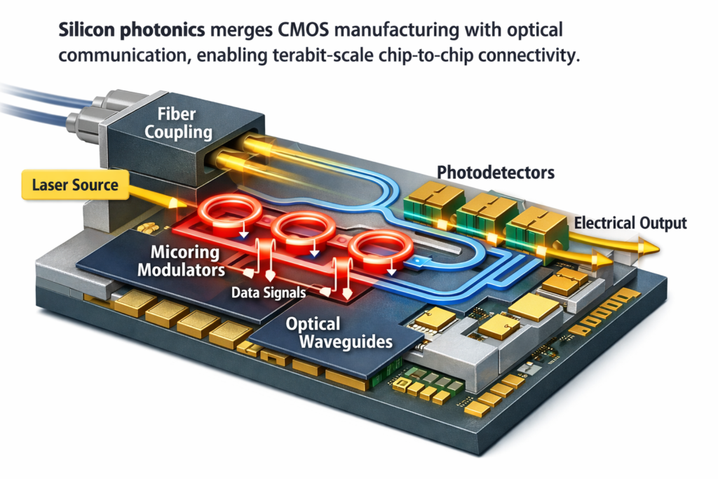
6.3 Silicon Photonics and Optical Computing
As electrical interconnects hit bandwidth-density walls (RC delays, power dissipation), silicon photonics offers light-speed communication.
Intel OCI (Optical Compute Interconnect):
- Integration: III-V lasers bonded to silicon photonics PIC (Photonic Integrated Circuit)
- Bandwidth: 4 Tbps bidirectional (first generation)
- Reach: Standard single-mode fiber, kilometers
- Co-packaging: OCI chiplets alongside CPUs/GPUs
Technical Implementation:
- DWDM (Dense Wavelength Division Multiplexing): 8+ wavelengths per fiber
- Microring resonators: Wavelength-selective modulation/demodulation
- Hybrid integration: Indium Phosphide lasers on Silicon substrates
Chapter 7: The Future Trajectory (2025–2035)
7.1 Roadmap to 1nm and Beyond
The semiconductor industry targets sub-1nm nodes (equivalent) through:
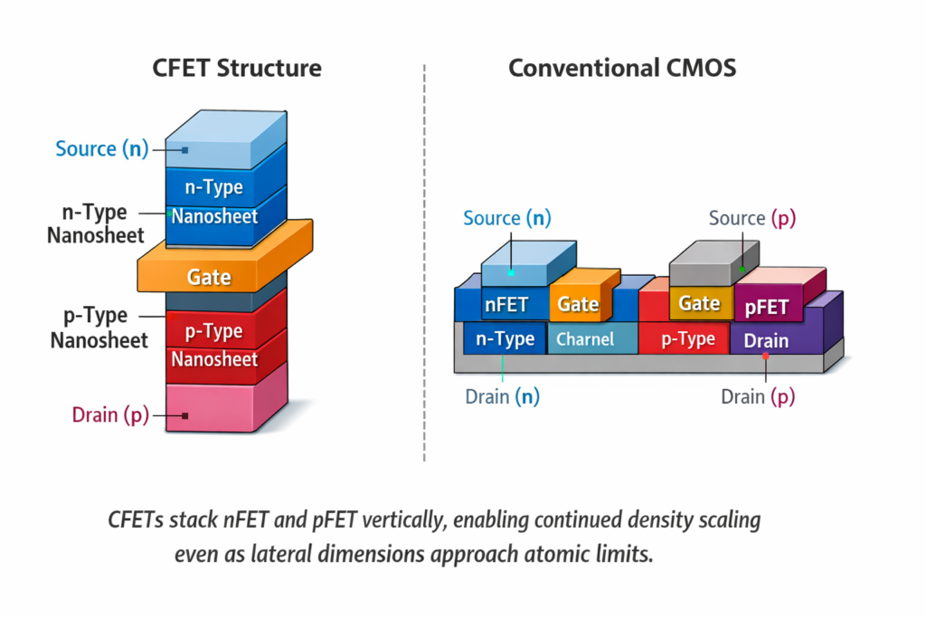
Complementary FETs (CFETs): Stacking nFET and pFET vertically (GAA-on-GAA) to reclaim CMOS footprint:
- Structure: n-type nanosheets above p-type nanosheets (or vice versa)
- Advantage: 50% area reduction versus side-by-side CMOS
- Challenge: Thermal management of stacked heat sources
2D Materials: Transition metal dichalcogenides (TMDs) like MoS₂ offer:
- Atomic thickness: 0.6-0.8nm monolayers
- Bandgap: 1.2-1.9 eV (suitable for logic)
- Mobility: Comparable to silicon at atomic scale
- Challenges: Contact resistance, defect density, large-area growth
7.2 Sustainable Computing
The energy consumption of AI training (GPT-4 required ~50 GWh) drives sustainable semiconductor innovation:
Approaches:
- Near-threshold computing: Operating at Vdd ≈ Vth for 10× energy efficiency
- Approximate computing: Accepting computational errors for non-critical applications
- Advanced cooling: Immersion cooling reducing datacenter PUE (Power Usage Effectiveness)
- Photonic interconnects: 10× better energy-per-bit than electrical I/O
Conclusion: The Never-Ending Story
The evolution of computer chips represents a triumph of human ingenuity over physical limitations. From the 2,300 transistors of the Intel 4004 to the 184 billion transistors of Apple’s M3 Ultra, we have witnessed a 100-million-fold increase in integration density. Yet this journey reveals a fundamental truth: when one scaling vector exhausts (Dennard scaling, planar transistors, monolithic integration), innovation shifts to new dimensions (parallelism, 3D architectures, specialized computing).
The next decade promises equally revolutionary changes. Gate-All-Around transistors will extend CMOS to 2nm and beyond. Advanced packaging will make the “chip” a system of systems. Neuromorphic and quantum processors will handle workloads impossible for von Neumann architectures. And new materials—2D crystals, topological insulators, superconductors—may redefine what a transistor even means.
For the AI/ML engineer, understanding this evolution is not academic curiosity—it is essential context. The algorithms we design run on physical substrates with specific constraints (memory bandwidth, power budgets, thermal limits). The most elegant neural network means nothing if it cannot be efficiently executed on available silicon. As we stand at the cusp of post-Moore computing, the symbiosis between algorithmic innovation and hardware capability has never been more critical.
The sand has been transformed. The revolution continues.